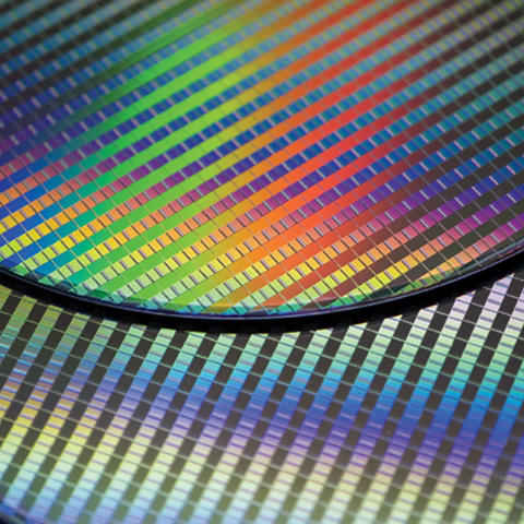
TSMC announces production plans for 5nm chips, possibly coming in 2020

TSMC 5nm chips are now in risk production
5nm chips to yield 15 percent performance gains over 7nm
Taiwan Semiconductor Manufacturing Company (TSMC) has just announced that the company has started the risk production of 5nm chips and would go into mass production by the first half of 2020. Additionally, the company has said they would start production of 5nm+ chips by 2021.
The new 5nm chips will be almost 45 percent smaller than the current 7nm chips and yield up to 15 percent performance gains without accounting for any architecture changes. The 5nm+ process would further improve upon these numbers by also delivering 6-12 percent better power efficiency. If the risk production goes as well as TSMC would hope, then it already has a number of potential customers lined up. These would include companies like Apple, for whom TSMC is the sole supplier till 2020, and maybe even Qualcomm, who used TSMC’s 7nm process for the Snapdragon 855. Given that Apple, Qualcomm and even HiSilicon would be expected to announce new flagship chips later this year, it is possible that one of them could be 5nm chips.
For those wondering, the difference between the 5nm and 5nm+ chips is in the lithography process. The lithography is the same size, meaning the chip still measures 5nm, but its process of fabrication is what’s different. The 5nm process uses a laser with the wavelength of 193nm to project a pattern onto the die through a mask. Since the wavelength is much bigger than the final node size, multiple masks have to be used in order to achieve the final 5nm node. The 5nm+ process instead will use Extreme Ultraviolet Laser (EUV Lithography) with a wavelength of just 13.5 nanometers, requiring very few masks as compared to the normal 5nm process. Producing EUV light is extremely difficult to achieve, not to mention expensive. Just to get some perspective, a EUV system contains over 100,000 parts, 40,000 bolts, 3,000 cables and 2 kilometers of hosing. One system also weighs 1,80,000 kilograms. While TSMC originally started its 7nm process using the longer wavelength lasers, the EUV method was designated with a + symbol, the production of which would start later. Samsung, on the other hand, had invested wholly into the EUV method.
Now that TSMC has announced its 5nm plans, we can expect something similar coming from Samsung in the near future.
Swapnil Mathur
Swapnil was Digit's resident camera nerd, (un)official product photographer and the Reviews Editor. Swapnil has moved-on to newer challenges. For any communication related to his stories, please mail us using the email id given here. View Full Profile


