Processor complexity will be limited only by molecule size now, says MIT

Imagine circuits built by molecules! Research by MIT has led to a breakthrough in self-assembling nanotechnology, which potentially has applications in silicon-based processor fabrication. By using specialized polymer-pairs and electron beam lithography, researchers found that the circuits on a processor can virtually build themselves, tremendously reducing manufacturing costs and allowing for a truly miniature-scale to the circuitry. While the technology is still quite a long way off from mass-scale production, its potential is staggering. Let’s have a look at how it works.

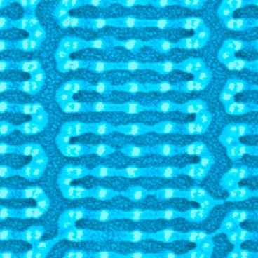
A view of the trenches created on a silicon wafer by a combination of copolymers, electron beam lithography, and nano-posts.
Current silicon-based processors are built layer by layer through a process called photolithography, where a layers of silicon, metal (or some other material) is deposited on a wafer, and then coated with a light-sensitive material called a photoresist. When this material is exposed to light, it hardens, so when the light is shone through a mask (stencil) with a detailed pattern on the photoresist, it hardens in the right spots, forming a circuit pattern. The unhardened material is then washed away, and chemicals are used to etch deeper grooves in the exposed surface of the chip.
This process of photolithography has been followed for more than 50 years, and now in the present day, we are fast approaching the limit of this process: the chips features are significantly smaller than the wavelength of the light used to create them. Manufacturers circumvented this barrier by ingeniously making light produce patterns smaller than its own wavelength, but as chips and their circuitry get smaller and smaller, this will not work anymore. An alternative that has been explored for years was to use self-arranging/assembling molecules to create the tiny circuits. MIT seems to have found a working solution to do just this.
Using electron beam lithography, patterns of nano-posts are made on the chip. These posts will then be deposited with special polymer pairs, which will interact with the posts to arrange themselves into useful preordained patterns themselves. As you may have guessed, the polymers are the most vital and enigmatic part of the process, along with the nanoscale posts. They are “copolymers,” or polymer pairs of two different types of polymer which intrinsically repel each other, but are forced to be together. When deposited on the sparse silicon “hitching posts”, the polymers will attempt to segregate themselves, and depending on the proportion of their lengths (polymers are chains of repeated organic molecules strung together) and types, they will take on a specific pattern.
After that, the process is simple, each polymer once in the desired pattern will be exposed to plasma, changing its state, i.e., the one which contains silicon will turn to glass, and the other will burn away. The resulting glass layer will be similar in effect to the photoresist from the photolithography process, and protect the layer beneath it while the rest is etched away.
Expect more transistors per chip than ever before, and even smaller, more energy efficient wafer sizes, that will make 32nm a thing of the past.
