New “microlaser” could help make smaller and more efficient chips

It seems that rules that can always be broken, and new paradigms can appear where there was previously no room for them. Recently, we brought you an piece on the latest copolymer and self-assembling nanotechnology research done by MIT, which had unarguable applications in the field of microprocessor fabrication. Why? It completely bypassed an age-old problem faced by chip-makers – of how to make trenches smaller than the wavelength of light used to create them – by using copolymers and nanoscale posts in a new method called electron beam lithography. While traditional photolithography circumvented this light-wavelength-barrier before by ingeniously making the light produce patterns smaller than its own wavelength, it could not have lasted for ever, as chips and their features got even smaller and more complex.
But now, with work done by the Quantum Optoelectronics Group at ETH Zurich, light will again be ingeniously used to make patterns smaller than its own wavelength, possibly heralding a new age for chip fabrication. Researchers, specifically Christopher Walther and 4 colleagues, have designed the world’s smallest electrically pumped laser, a microlaser, which is much smaller than the light it emits.

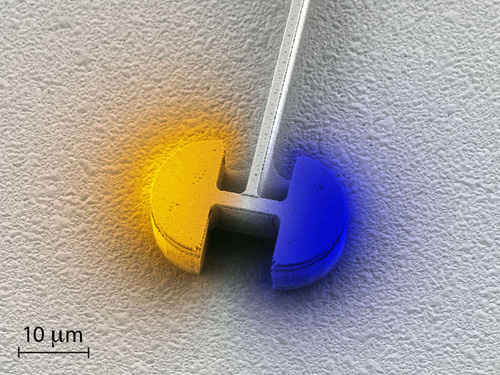
The centerpiece of the new microlaser is the electric resonator, consisting of two semi-circular capacitors that are connected via an inductor (here, a scanning electron microscope image). The color intensity represents the strength of the electrical field; the color itself, the respective polarity. (Photo: ETH Zurich)
The laser is 30 micrometers long and 8 micrometers high, producing a wavelength of 200 micrometers. It differs from conventional optical lasers by not having light travel back and forth between larger-than-its-wavelength-mirrors in optical resonator. Instead, using an “electrical resonant circuit made up of an inductor and two capacitors”, scientists can capture light in it, and produce a laser by inducing the light into self-sustaining electromagnetic oscillations using a optical amplifier. According to Walther, this means that “the size of the resonator is no longer limited by the wavelength of the light and can in principle…be scaled down to whatever size you want”.
About chip manufacturing possibilities, Walther goes on to say “If we manage to approximate the transistors in terms of size using the microlasers, one day they could be used to build electro-optic chips with an extremely high concentration of electronic and optic components”.
So, chip-makers have two viable options delivered to them by researchers from Zurich and MIT. Which one will they choose? Electron beam lithography has some advantages, at least in the short term, as it can be used to produce regular silicon-based processors instead of “electro-optic chips”, which are still on the drawing board of think tanks. It is also an extremely energy efficient method, with the self-assembling nanotechnology doing most of the work for them once they are properly stimulated.
