New 2D semiconducting material may lead to faster chips

The semiconductor material is made of tin monoxide that is only one atom thick, and was discovered by a team of engineers at the University of Utah
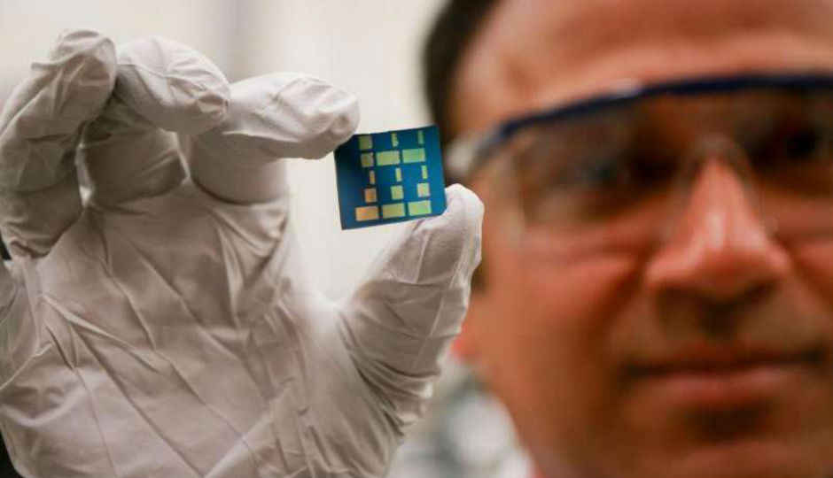
Engineers at the University of Utah have discovered a new kind of 2D semiconducting material that may lead to faster and more efficient computers and smartphones. The semiconductor is made of tin monoxide (SnO) and the layer of material is only one atom thick, which lets electrical charges move faster than conventional 3D semiconducting materials like Silicon. Currently, transistors and other components in devices are made using 3D materials on a glass substrate. In these materials, electrons have room to move in all directions inside the layers. With 2D materials however, the thickness of the layer is only about one or two atoms. This means that the electrons and only move in a single layer, so it is much faster. The team was lead by the university’s materials science and engineering associate professor, Ashutosh Tiwari.
While researchers have discovered other 2D materials like graphene, molybdenum disulphide, and borophene, these materials only allow the movement of N-type, or negative electrons. To create an electronic device, manufacturers require semiconductor material that will allow the movement of negative as well as P-type, or positive electrons. Tin monoxide is the first stable P-type 2D semiconducting material ever in existence. This discovery may lead to manufacturing of transistors that are even smaller and faster than the one being used today. Another benefit is that since the movement of the electrons is limited to just one layer, there will be less friction. This will lead to cooler chips that require less power to operate.
Source: Phys.org


