
India’s semiconductor chip manufacturing dream is no longer just etched in strategy papers or hollow government declarations. With talent pipelines being built and supply chains cautiously stitched together, it’s finally taking shape. Applied Materials is closely involved in this process, according to Dr. Suraj Rengarajan.
“We are fully aligned with India’s ambition to become a global semiconductor hub,” says Dr. Suraj Rengarajan, Head of the Semiconductors Product Group at Applied Materials India. “With over 20 years of experience in the country, we’re here not just to participate – but to help shape it.”
Also read: Intel’s India vision: From AI acceleration to enabling electronics manufacturing for the world
A recent report by ET indicates that the nation’s semiconductor market – valued at around US$52 billion in 2024 – is projected to more than double to over US$103 billion by 2030. This surge is fueled by robust initiatives like the US$10 billion India Semiconductor Mission and extended fiscal incentives aimed at fostering local manufacturing and reducing import dependency.
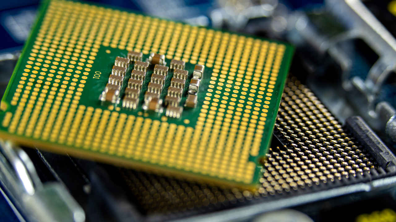
Applied Materials is one of those few names globally that matters in the building blocks of chips. Think precision machinery for nanoscale layering and etching, backed by decades of materials science, systems engineering, and process tech. Now they’ve cast their lot firmly with India.
India’s semiconductor chip manufacturing sector has challenges
Because let’s face it, building semiconductor manufacturing capacity in India was never going to be easy. It’s a generational moonshot. What sets Applied’s approach apart, according to Dr. Rengarajan, is their integrated play that brings together infrastructure, innovation, supply chains, and most critically – talent.
In 2023, they launched the Applied Materials Innovation Center for Semiconductor Manufacturing. But that’s not just a facility with fancy acronyms – it’s a signal, he says. “The center is designed to accelerate the development and commercialization of semiconductor equipment technologies, while building a strong local supply chain,” Dr. Rengarajan explains.
Also read: AMD’s Jaya Jagadish: India to play ‘transformative role’ in global AI, datacenter and chip landscape
And then there’s the India Validation Center, or IVC. Located in Bengaluru, it’s the first private industry facility in India capable of processing 300-mm wafers. Let that sink in. It’s a cornerstone move. Because without the ability to simulate, test, and validate chip-making tools, you’re not really building for scale – you’re just trialing in theory.
Applied’s investments are deliberate, and deeply layered. The IVC supports not just Applied’s global roadmap, but for creating a sandbox for Indian fabs, startups, and researchers to plug into.
Creating Indian silicon manufacturing talent pool is key
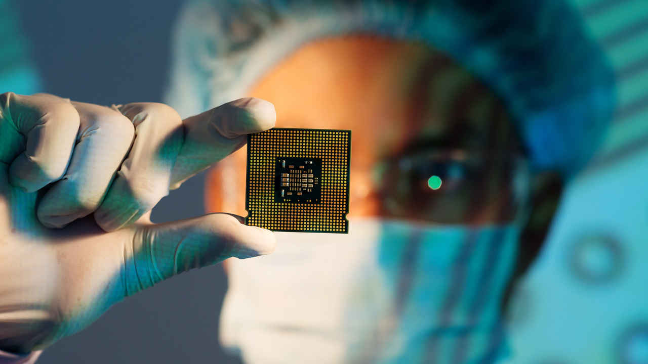
But chips don’t make themselves, and machines certainly don’t run themselves. At the heart of this entire movement is talent. And that’s where Applied is doubling down in ways that are quietly powerful.
“Talent development is a crucial component,” says Dr. Rengarajan. “That’s why we’ve partnered with IIT Bombay, IISc, IIT Patna, and IIT Ropar. We want to offer students hands-on experience and direct exposure to industry leaders.”
The company’s 18-year partnership with IIT Bombay has yielded not just research breakthroughs but actual labs on campus – NanoElectronics and Chemistry & Materials Sciences – and the first-of-its-kind semiconductor certification course. And with the ASCENT program (Applied Semiconductor Collaboration in Engineering and Technology), they’re building bridges between faculty, students, and working professionals to take academic curiosity to real-world readiness.
A particularly notable development is the AI-enabled Centre of Excellence Applied Materials is setting up in Chennai, in partnership with the Tamil Nadu government.
“This center will serve as a hub for applying AI and advanced analytics to optimize semiconductor manufacturing processes and equipment design,” Dr. Rengarajan shares.
The timing is no coincidence. With AI and IoT becoming the major growth engines of chip demand, the manufacturing backend needs to scale up in sophistication. From defect detection to material discovery, AI is transforming how chips get made. And Applied is betting that India can be one of the places where this next wave of innovation is not just consumed – but conceived.
Take the SEMVision H20, one of Applied’s advanced systems. It combines electron beam tech with AI-driven image recognition to detect nanoscale defects buried deep inside advanced chips. That’s not just cool tech, but core to making sure your AI model doesn’t crash when you fire up your phone.
India’s local supply chains: The missing link
As much as everyone loves the idea of India becoming the next Taiwan or Korea of chipmaking, there’s still a missing piece: domestic supply chain muscle. Applied Material’s been quietly working on that too.
“We are collaborating with global suppliers from the U.S., Europe, and Japan to help them establish operations in India,” says Dr. Rengarajan. “We’re also working with local suppliers to help them meet industry standards and qualify for fab infrastructure and equipment manufacturing.”
Also read: AI chips and Indian innovation: Insights from Tessolve CEO Srini Chinamilli
This is how you do it. Not by just making a checklist of which parts are needed for a fab, but by actually building a web of incentives, training, and quality processes so that parts don’t just arrive – they get made here. From specialty gases to spare parts and ultra-pure chemicals, the devil’s in the industrial detail.
And those collaborations? They aren’t just transactional. “Through our Validation Center and other infrastructure, we’re co-developing next-gen semiconductor equipment with suppliers,” Rengarajan notes. “That partnership accelerates innovation across the ecosystem.”
IoT and AI are fuelling the appetite for chips
If chips were once about smartphones and laptops, that world is fast expanding. The next big wave is already here: AI inference chips, IoT edge nodes, electric vehicle controllers, and more.
“The rise of IoT and AI marks the beginning of the fourth and largest era of computing,” says Dr. Rengarajan. “They will demand more specialized chips, advanced packaging, and robust security features. That’s where manufacturers will need to innovate rapidly.”

And Applied Materials isn’t just building for that future – it’s living it already. Internally, they’re deploying AI to modernize ERP, optimize their own processes, and transform operations. It’s not enough to build the tools – you have to use them too.
The Chennai Center of Excellence isn’t just another lab. It’s a proof of the fact that India isn’t just an assembly line for products, but an innovation zone and breeding ground of future tech.
We all know that India’s been a late bloomer in the semiconductor game, mostly content to lead in software, services, and some chip design. But as geopolitical winds shift, the country is finally betting big on becoming a manufacturing powerhouse in high-tech sectors, too.
There’s a reason why the India Semiconductor Mission (ISM) is putting down ₹76,000 crore in incentives. And there’s a reason Applied Materials is putting boots on the ground and tools in the lab. “This is India’s time to shine,” Dr. Rengarajan says. “We’re excited to accelerate the journey from vision to reality.”
What’s clear is that Applied Materials isn’t here for a press release. They’re here for the long haul. They’re not just building for India, but building with India, emphasises Dr. Rengarajan.
Message to future Indian chipmakers
So what’s the takeaway for young engineers reading this? For those wondering whether to get into chips instead of coding one more SaaS app?
Dr. Rengarajan’s message is hopeful and direct: “Imagine being at the forefront of a technological revolution, shaping the future of both India and the world. That’s the exciting opportunity awaiting students and professionals in the semiconductor sector.”
If you’re into chip design, materials science, AI-driven optimization, or just want to be where the future’s being soldered together – there’s space for you.
“Now is the perfect time to dive into semiconductors,” he adds. “The opportunities are vast, and your contributions will help place India at the forefront of the global semiconductor landscape.”
Also read: Future of Computing in 2025: Top 6 innovations shaping tomorrow’s tech
Jayesh Shinde
Executive Editor at Digit. Technology journalist since Jan 2008, with stints at Indiatimes.com and PCWorld.in. Enthusiastic dad, reluctant traveler, weekend gamer, LOTR nerd, pseudo bon vivant. View Full Profile