When it comes to semiconductor chip companies, it’s hard to look beyond the obvious choices like Intel, AMD, TSMC, NVIDIA, Qualcomm, MediaTek and Samsung. But ask any of these big chip companies, and they’ll be the first ones to tell you that they are supported by an army of partners in bringing all the pieces of the semiconductor chip jigsaw puzzle together. Tessolve is one such important player in not just India’s but the global chip design and manufacturing industry.
According to the Co-Founder and CEO, Srini Chinamilli, Tessolve’s expertise lies in semiconductor and embedded technologies. “From smartphones and wearables to critical systems in automotive, industrial, and avionics sectors, our services are integral to the semiconductors powering these innovations,” he says.
Also read: Intel launches powerful Xeon 6 and Gaudi 3 AI chips amid stiff competition
Founded in 2004, Tessolve is a multinational semiconductor engineering solution provider headquartered in Bangalore, India. The company serves a diverse customer base, including leading semiconductor manufacturers and technology companies. “We have designed parts for an interesting touch-sense application for SigmaSense, made SOMs with Renesas parts for industrial robots, systems for 2-wheeler dashboards, and even IOT devices for Kaapi Machines,” explains Chinamilli, to showcase some of the work they’ve been doing recently, among other things. Tessolve’s had a hand in designing components for everything from industrial robots to IoT devices for coffee machines. But what truly sets them apart is their end-to-end approach – covering chip design, testing, product engineering, and system design – all under one roof.
As AI becomes more woven into the fabric of our everyday lives, I wanted to delve into how Tessolve is navigating the complex landscape of AI chip development. And perhaps, most intriguingly, how does Tessolve see India’s role in the global semiconductor arena, especially as the country positions itself as a burgeoning hub for tech innovation? I posed these questions and more to Srini. His insights offer a fascinating glimpse into the future of technology and the pivotal role companies like Tessolve will play in shaping it. Edited excerpts follow:
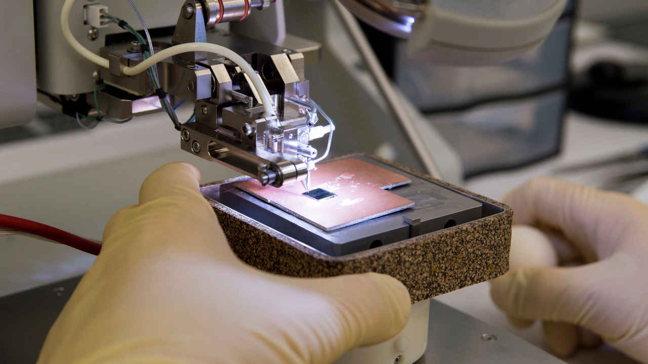
As an intricate and highly specialised process that many people may not fully appreciate, semiconductor chip manufacturing involves multiple testing stages, validation, optimization, and reliability to ensure performance. The importance of these steps are to ensure proper performance, to the point where a minor defect can lead to significant issues in the final product, across different conditions is often overlooked.
At Tessolve, while we do not manufacture chips, our critical role comes in with the comprehensive design, testing, and validation of the process, with our expertise spanning initial chip design to post-silicon validation to ensure that each chip meets the highest quality and reliability standards prior to market-entry to meet the demands of industries like AI, automotive, and telecommunications, where reliability is crucial. To maintain these standards, we use advanced testing platforms capable of simulating real-world conditions, allowing us to detect and address potential issues early in the development cycle. Our engineers work closely with chip manufacturers to optimise designs for performance, energy efficiency, and scalability.
Tessolve has evolved significantly since its establishment in 2004. We initially identified a gap in India’s semiconductor testing and productization capabilities, which motivated us to build world-class engineering teams. Today, Tessolve has grown into the largest standalone semiconductor solutions provider, with over 3,000 engineers across 10 countries.
Along with an end-to-end service model, covering everything from chip design and testing to product engineering and systems design, our deep expertise in ARM-based SOCs, HSIO (high speed IO), managing 500w+ devices, and testing for defects at 3nm differentiates us from other engineering service providers in the industry, positioning us as a key player in advancing semiconductor technologies worldwide.
With the rapid rise of AI chips, the complexity of design and testing has grown significantly. To stay at the forefront of these advancements, Tessolve has established a Center of Excellence focused on cutting-edge technologies to ensure we are well-prepared to meet the demands of emerging technologies.
Also read: From IIT to Infosys: India’s AI revolution gains momentum, as 7 new members join AI Alliance
AI chiplets, in particular, have become increasingly important, and we have invested heavily in enhancing our design capabilities for Design Verification for UCIe interface (this is almost a must-have) chiplet DFT, advance packaging for silicon interposers, and testing. We’ve also invested in the latest testers capable of handling the complexities of AI chip testing. These strategic investments are already yielding positive results and positioning us as a key player in the evolving AI landscape.
At Tessolve, we’ve focused on key advancements in AI chips by enhancing analog designs for high-performance IVRs, and significantly improving our ATE capabilities and data collection. Our expertise in high-power device testing and reliability through ATE has been crucial, especially for advanced nodes and high-power applications. We’ve also led the way in UCIe package designs, driving innovation for scalable ARM-based SoC solutions, while ensuring reliability and performance.
Tessolve has formed strategic partnerships with AI chip designers and industry leaders, functioning almost like their extended engineering arm, spanning across the entire product lifecycle, from chip design to post-silicon testing, and product engineering. Through our collaboration with companies like SigmaSense and Renesas, we have developed advanced solutions for various applications such as industrial robotics. Our expertise in AI chiplet design, high-power device testing, and UCIe interfaces, when combined with these key partnerships, help us deliver groundbreaking innovations and deliver highly specialised AI solutions tailored to industry needs.
At Tessolve, we believe in the philosophy that every disruptive technology presents a unique set of challenges and viewing them as opportunities is the key to sustain the organisation in the long run. Presently, one of the major challenges we are facing in the AI chip domain is the rising cost of advanced technology development. Additionally, ensuring that our engineers possess the necessary skills to adapt to rapidly evolving technologies is also demanding. However, we strongly believe that the opportunities outweigh the challenges with AI driving the demand for sophisticated chips, which has boosted the need for design, testing, and validation services.
This provides significant growth and expansion opportunities for Tessolve, with the increasing volume of designed and tested AI chips presenting a thriving business landscape. Our focus remains on seizing these opportunities, staying at the cutting edge of innovation, and continuing to support the industry’s growing needs, positioning ourselves for sustained success in this evolving field in the process.
As AI continues to evolve, the semiconductor industry is at a major inflection point, with new standards and approaches being established. Leading companies – such as Tesla, Google, Microsoft, and Ola – are now focusing on developing their own custom silicon, underscoring the trend of the growing importance of chip design in national and global ecosystems. If data was once considered the new oil, then chips have become the new data, driving innovation and competitive advantage across industries.
Also read: From DLI to AI: Cadence talks India’s chip design efforts
At Tessolve, we are positioned for accelerated growth as this shift towards custom silicon deepens, as companies developing their own AI chips will increasingly seek the support of partners like us, who bring expertise at scale in design, testing, and development. This surge in demand for customised solutions will require more testing and the need for skilled engineers, which will not only drive Tessolve’s growth but also contribute to the advancement of the broader industry.
At Tessolve, our R&D efforts are centred around next-generation AI chip technologies, focusing on developing innovative testing methodologies for highly complex AI chips. By leveraging automation and innovative testing methodologies to improve chip performance, we have equipped ourselves to meet the increasing demand for AI chips across sectors like automotive and datacenters. Through AI-driven testing and development processes, we are advancing AI chip technologies. These chips, often featuring large die sizes and deep submicron manufacturing processes, require advanced testing techniques to address challenges such as fault detection, shrinking geometries, high-speed interfaces and ultra-high-power consumption. These R&D efforts also support emerging technologies like AI accelerators, HBM, IoT, and 5G, ensuring reliability, performance, and low power consumption across various applications.
We have been a part of India’s semiconductor landscape for over 20 years, setting up the country’s first state-of-the-art semiconductor test and qualification labs, and training over 5,000 engineers to build India’s growing semiconductor ecosystem from the ground up. With the government’s increased focus on semiconductor manufacturing, we are poised to play a significant role in supporting new product companies and manufacturing facilities. Our extensive engineering capabilities, spanning chip design to system-level solutions, will be instrumental in supporting India’s ambitions to become a global semiconductor hub.
Having invested in advanced technologies and engineering solutions, Tessolve has significantly contributed to India’s growing semiconductor manufacturing ecosystem. Our experience in test and product engineering, design, and system integration has positioned us to support global and local consumers.
For Indian entrepreneurs looking to make their mark in the semiconductor industry, my message is clear: you are in the right place at the right time. The next few decades will be India’s opportunity to lead, and entrepreneurs like you will define this journey. The beauty of today’s landscape is that one needn’t necessarily invest in large manufacturing setups to bring their ideas to life. If you have an innovative concept, Tessolve is here to help with the design and testing of your chip, leveraging our collaborations with packaging companies and chip manufacturers to turn your ideas into reality.
My advice to young entrepreneurs is to focus on innovation and seek partnerships with experienced industry players. At Tessolve, we are committed to supporting you in this journey and helping you navigate the complexities of semiconductor design and development to shape the future of India’s semiconductor industry together.
Also read: How computer vision and AI will automate toll booths on Indian roads and highways